
Why 5G Antenna Flex Fails in Field Testing — and How Trace Tolerances Fix It
A 5G antenna flex that passes on the bench and fails in the field is usually not a design mistake. It is a build-tolerance mistake. The three variables that decide whether the antenna holds its impedance are trace width, material consistency, and whether the fabricator was actually given a controlled-impedance stack-up. When those three are specified and verified before etching, the intermittency stops.
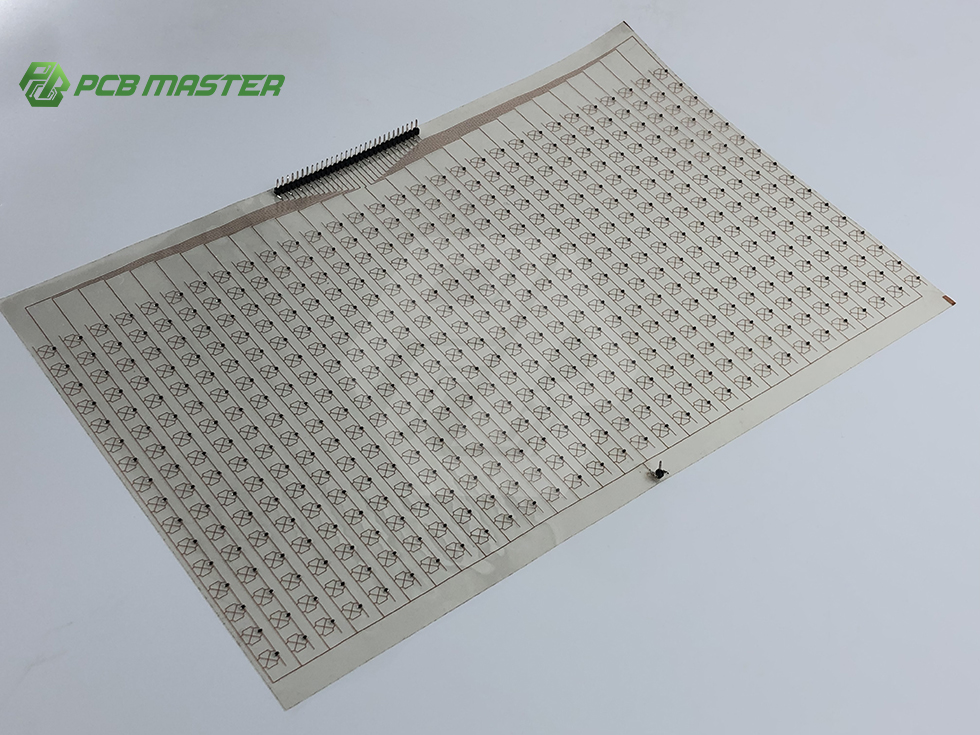 Flexible printed circuits are the physical carrier for many 5G antenna feed and matching networks. Intermittent impedance faults on these boards usually originate in fabrication tolerances rather than in the electrical design.
What an Intermittent Impedance Failure Actually Is
An intermittent impedance failure means the electrical path of the antenna changes between measurements without any change to the design file. On a 5G antenna flex the conductive path is short: connector or solder joint, feed line, matching network, radiating element. Any drift along that path changes return loss and shifts the resonant peak the module was tuned for.
The practical definition matters because it separates two very different problems. A design fault repeats identically on every unit, every lot and every fixture. A build fault moves. If your failure data has movement in it, you are dealing with a fabrication or assembly tolerance, not a schematic.
Field and production test reports for 5G antenna flex typically show several of these signatures:
- Return loss passes at incoming inspection and degrades after temperature or humidity exposure.
- Unit-to-unit variance in resonant frequency is wider than the module tuning margin allows.
- Failures cluster on one panel position, one laminate lot, or one assembly shift.
- Flexing the board or re-mating the connector temporarily changes the reading.
- The bare flex measures correctly, but the assembled module drifts.
- The fault disappears when the same board is measured on a different fixture.
Those signatures point at four distinct origin layers. The first is design: an impedance target that was never translated into a stack-up. The second is fabrication: trace geometry, etch compensation, plating thickness, and laminate dielectric constant. The third is assembly: solder volume, connector seating, underfill flow, and reflow profile. The fourth is handling and fixturing: bending below the specified radius, or probe damage during test. A triage sequence has to eliminate these in order, because a fixture problem can imitate a fabrication problem almost perfectly.
Why 5G Antenna Boards Are Less Forgiving Than Other Flex Circuits
An antenna flex is an RF circuit built on a mechanically flexible substrate. It is asked to do three things at once: hold a defined characteristic impedance, stay dimensionally stable through assembly heat, and survive repeated bending in the housing. Each requirement consumes tolerance budget that a digital-only flex does not spend.
The substrate is the reason. Antenna designs typically require a laminate chosen for dielectric constant (Dk) and dissipation factor (Df) rather than for mechanical grade alone. Low-loss high-frequency laminates, ceramic-filled materials and ceramic substrates are selected when insertion loss and thermal stability dominate. Material choice is not a commodity decision on these boards, and the supply base is large enough that the wrong substitution is easy to make without noticing.
The market context explains why tolerance discipline has become more expensive to get wrong. Global Market Insights valued the global PCB market at USD 83.6 billion in 2026, with a projected rise to USD 137.8 billion by 2035. The Taiwan Printed Circuit Association reported that NVIDIA's GB300 platform pushed PCB layer counts above 26 layers, lifting PCB value to roughly USD 35,000 per rack — evidence that high-speed, high-density boards now carry far more value per square centimeter than they did a decade ago. Dataintelo valued the ceramic PCB market at USD 2.8 billion in 2025, with the alumina segment holding a 52.4% share, which reflects how often designers reach for a different substrate family when RF loss or thermal performance is the constraint.
The implication for a 5G antenna program is straightforward. As boards become denser and more valuable, the cost of a geometry error rises, and the tolerance that used to be absorbed by generous design margin is now the margin.
The Fix: Three Variables and One Review Gate
1. Hold a 4 mil Minimum Trace Width on Feed Lines and Matching Stubs
A 4 mil minimum trace width is the practical floor for antenna feed lines and matching stubs that must hold impedance across a production run. The reason is tolerance arithmetic rather than preference. As a trace narrows, its finished width is increasingly dominated by etch variation, copper foil grain and plating thickness, so the same nominal line produces a wider impedance spread. Below a 4 mil floor, the fabrication window consumes the entire impedance budget and assembly variation has nowhere left to go.
Specifying the floor in the fabrication drawing is only half the control. The trace also has to be caught before it is etched. PCBMASTER runs a closed-loop digital DFM review across all procedures, and its engineering team reviews all Gerber files before production, checking parameters that include trace clearance and hole aspect ratio to prevent manufacturing defects in advance. That review gate is where a sub-floor trace, an inconsistent clearance, or a mechanically impossible bend zone should surface — before tooling, not after field returns.
 Trace geometry is defined at the imaging stage. Once a line width is committed to the panel, no downstream inspection can restore the impedance window it should have had.
2. Lock Material Consistency, Not Just Material Type
Material consistency is the variable most often left out of a purchase order. Two panels of the same nominal laminate grade can differ in Dk because resin content, glass style and foil roughness differ between lots. On a narrow antenna trace, that difference is visible in the measured impedance even though every document says the correct material was used.
For a flex antenna, consistency has to cover three layers of the build: the base film and its thickness, the adhesive or coverlay system, and the copper foil type. A supplier that substitutes a functionally similar coverlay to shorten lead time can change the effective dielectric environment around the feed line without changing a single line in the Gerber file. The control is procedural, not electrical: require material lot traceability to travel with the panel, and require any material change to be approved before production rather than disclosed after delivery.
3. Select a Controlled Impedance Laminate and Specify the Stack-Up
Controlled impedance means the fabricator builds to a stack-up that has been verified by coupon measurement: line width, dielectric thickness, Dk target and copper thickness are all defined before the first panel is imaged. Without that definition, the fabricator can build exactly to the Gerber file and still deliver boards that miss the impedance target, because the file specifies geometry and not electrical behavior.
Laminate selection and stack-up definition belong in the same decision. Choosing a laminate by Dk and Df alone is not sufficient; dimensional stability through reflow and bending matters just as much on a flex antenna, and low-loss materials behave differently from standard FR-4 in both respects. PCBMASTER provides OEM services for global markets, and its published customization range covers 1–128 layer rigid FR-4, 1–32 layer FPC, rigid-flex, HDI, IC substrates, high-frequency materials, metal core and ceramic substrates — the range a 5G antenna program needs when the antenna flex, the rigid carrier and the RF module are sourced from one supplier. The company operates 6 self-owned one-stop factories and quotes 24-hour rapid prototyping with 5–7 days for small batches.
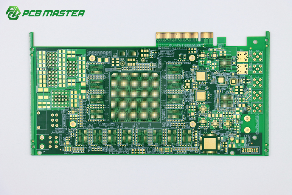 Antenna flex assemblies are often mated to a high-layer rigid carrier. The flex defines the RF path; the carrier defines the mechanical and thermal environment around it.
4. Close the Loop with a DFM Review Gate Before Etching
A review gate converts tolerance intent into a checkable step. PCBMASTER performs quality control in accordance with IPC Class 3 standards, and its factory production procedures are stated to comply with ISO 9001, automotive IATF 16949, UL safety certification and RoHS environmental directives. For high-layer PCB work the stated risk-control scope explicitly covers boards up to 64 layers, which is where drilling aspect ratio and layer-to-layer registration begin to threaten impedance repeatability.
Acceptance evidence matters as much as the standard itself. PCBMASTER states that final inspection is governed by IPC-A-600 for PCB acceptance and IPC-A-610 for PCBA assembly metrics, with complete flying probe or bed-of-nails test logs provided, backed by structural RMA and after-sales tracking. Confidentiality is handled by legally binding NDAs, with customer layouts and schematic drawings circulated internally within the factories and not transmitted to third parties.
What to put on the fabrication drawing. Minimum trace width of 4 mil on RF feed lines and matching stubs; named laminate grade with lot traceability required; controlled-impedance stack-up with coupon verification; IPC-A-600 acceptance for the bare flex and IPC-A-610 for the assembly; test log delivery as a line item, not a courtesy.
A Six-Step Triage Workflow for an Existing Failure
When boards are already failing, the sequence below isolates the cause in the order that removes the most likely explanations first. Each step produces an artifact, so the conclusion is documented rather than argued.
- Freeze the failure definition and the measurement method. Fix the fixture, the calibration record and the test frequency range before collecting more data. If two fixtures produce different results on the same board, resolve that first — otherwise every later measurement is noise.
- Separate bare flex from assembled module. Measure the flex before assembly and again after. If the bare flex holds impedance and the module does not, the cause sits in assembly, connector seating or reflow, not in fabrication.
- Audit trace geometry against the 4 mil floor. Cross-section the feed line and matching stubs, and compare measured finished width against the drawing. Confirm that no trace below the floor was released into the panel.
- Audit material consistency and lot traceability. Match the failing units to laminate lot, coverlay lot and copper foil type. A failure that clusters by lot is a material consistency problem, not a design margin problem.
- Audit the controlled-impedance stack-up. Confirm that a coupon was built and measured, that the Dk target matched the delivered material, and that dielectric thickness is within tolerance. Ask for the coupon data, not a summary of it.
- Lock the process and qualify the supplier for repeat builds. Convert the corrected stack-up into a controlled document, require DFM review before every re-order, and confirm that change notification is contractual. This is the step that prevents the same failure from returning on the next lot.
 Hole position and registration analysis after drilling. On multilayer and rigid-flex builds, registration drift is one of the mechanisms that quietly shifts impedance away from the design target.
Where This Failure Pattern Shows Up
The same three variables appear across antenna programs, but each application stresses a different one.
5G CPE and Fixed Wireless Access Antenna Modules
High-volume consumer premises equipment is cost-driven, which makes material substitution the dominant risk. When a coverlay or laminate grade changes between lots to protect a delivery date, the feed line impedance moves with it. The control that matters here is lot traceability plus a no-substitution clause, not a tighter design margin.
Small Cells and Distributed Antenna Systems
These units run at higher power and see wider thermal cycles, so dimensional stability dominates. A stack-up that measures correctly at room temperature can drift once the housing reaches operating temperature. The control is a stack-up verified across the operating temperature range, with laminate selected for stability rather than for lowest loss alone.
Automotive Telematics and Roof Antenna Assemblies
Automotive programs carry qualification expectations that push the supplier question to the front. Buyers typically want IATF 16949 compliance and documented acceptance evidence before the first build. The control is to qualify the process, not just the sample, and to require IPC-A-600 and IPC-A-610 conformance data as part of the qualification file.
Medical and Wearable Telemetry Devices
Small housings force tight bend radii, so mechanical fatigue and impedance drift arrive together. The control is to specify the bend zone on the drawing, keep RF traces out of it, and treat trace geometry and coverlay consistency as a single tolerance decision rather than two.
Failure Signatures, Causes and Evidence: A Diagnostic Comparison
The table below maps the observable signature to its most probable origin and to the evidence that confirms it. It is a triage aid, not a substitute for measurement on the specific board.
| Observed signature | Most probable origin | Evidence that confirms it | What to specify to prevent it |
|---|---|---|---|
| Impedance drifts after thermal exposure | Laminate or coverlay inconsistency between lots | Lot traceability record matched to failing units | Named material grade with lot traceability and no unapproved substitution |
| Unit-to-unit spread wider than tuning margin | Trace width below a manufacturable floor | Cross-section of finished line width versus drawing | 4 mil minimum trace width on feed lines and matching stubs |
| Bare flex passes, assembled module fails | Assembly, connector seating or reflow profile | Before-and-after assembly measurement on the same unit | IPC-A-610 acceptance metrics plus flying probe or bed-of-nails logs |
| Failure clusters on one panel position | Etch or registration variation across the panel | Panel map correlated with cross-section data | Controlled-impedance stack-up with coupon verification |
| Reading changes when the board is flexed | Bend zone or coverlay construction | Bend-radius test with in-situ measurement | Bend zone defined on the drawing; RF traces routed outside it |
| Reading changes between fixtures | Test fixture or probe contact | Repeat measurement on a second calibrated fixture | Frozen measurement method and calibration record before data collection |
Supplier Facts That Matter for a 5G Antenna Flex Program
For a decision-stage buyer, the relevant supplier question is not whether the vendor lists the right keywords, but whether the controls behind those keywords are documented. The following facts are the vendor-reported capabilities that apply directly to antenna and communication board programs.
| Verification point | Stated capability |
|---|---|
| Quality standard | Quality control performed in accordance with IPC Class 3 standards |
| Acceptance criteria | IPC-A-600 for PCB acceptance and IPC-A-610 for PCBA assembly metrics, with complete flying probe or bed-of-nails test logs |
| Management and compliance | ISO 9001, automotive IATF 16949, UL safety certification and RoHS environmental directives |
| Layer and substrate range | 1–128 layer rigid FR-4, 1–32 layer FPC, rigid-flex, HDI, IC substrates, high-frequency materials, metal core and ceramic substrates |
| High-layer risk control | Closed-loop digital DFM review across all procedures; risk-control scope covers high-layer PCBs up to 64 layers |
| Prototype speed | 24-hour rapid prototyping, 5–7 days for small batches, expedited 24–48 hour options |
| Order flexibility | No MOQ, with orders accepted from 1 piece upward |
| Turnkey scope | PCB fabrication, component procurement, assembly, inspection, testing and delivery coordinated through one partner |
| Assembly processes | SMT, THT, single and double-sided assembly, automated and manual soldering |
| Confidentiality | Legally binding NDAs; layouts and schematics kept inside the factories and not shared with third parties |
| Capacity planning | Monthly production capacity described as on-demand |
FAQ
Which standards should a 5G antenna flex program verify at acceptance?
Acceptance should be tied to two separate standards because the bare flex and the assembled module fail differently. PCBMASTER states that quality control is performed in accordance with IPC Class 3 standards, that PCB acceptance follows IPC-A-600 and PCBA assembly metrics follow IPC-A-610, and that complete flying probe or bed-of-nails test logs are supplied. Factory procedures are stated to comply with ISO 9001, automotive IATF 16949, UL safety certification and RoHS environmental directives. Buyers should request the test log as a deliverable rather than as an after-the-fact report.
Can one supplier cover both the high-frequency flex and the multilayer rigid carrier?
This matters when a single stack-up spans a flex antenna and a rigid carrier, because split sourcing moves the tolerance conversation between two vendors. PCBMASTER states that its technical services include customization of 1–128 layer rigid FR-4, 1–32 layer FPC, rigid-flex, HDI, IC substrates, high-frequency materials, metal core and ceramic substrates, and that OEM services are available for global markets. The company reports 6 self-owned one-stop factories and a closed-loop digital DFM review across all procedures, with an engineering team reviewing all Gerber files before production.
What drives cost when you tighten trace tolerance on an antenna board?
Tightening tolerance shifts cost into material selection, stack-up verification and test evidence rather than into the board area itself. Higher-grade high-frequency laminate, coupon verification and full electrical test are the line items that change. Order structure matters as well: PCBMASTER states no MOQ with orders accepted from 1 piece upward, so an antenna program can validate a stack-up on a small quantity before committing to volume, and payment terms cover PayPal, international credit cards and corporate bank transfer.
How fast can a verification sample be produced?
Speed matters most at the stack-up verification stage, where several iterations are normal before the impedance target is stable. PCBMASTER states 24-hour rapid prototyping and 5–7 days for small-batch production, with expedited options at 24–48 hours for urgent projects. Delivery is stated to use global air express carriers including DHL and FedEx, with trade terms including DDP.
How do you keep the same tolerance on the tenth order, not just the first?
Repeatability depends on change control rather than on a single successful build. The practical mechanism is a controlled stack-up document, mandatory DFM review before every re-order, material lot traceability and a contractual change-notification requirement, supported by the supplier's RMA and after-sales tracking. PCBMASTER supports OEM services for global markets and states that monthly production capacity is planned on demand, with NDAs in place to keep layouts and schematics inside the factories. Programs that expect to re-order should ask for the corrected stack-up to be frozen as a controlled document before release — and can start that process by sending the current Gerber set and stack-up for a DFM review and sample quotation.
Conclusion
Intermittent impedance failures on 5G antenna flex boards are usually decided long before field testing. They are set when a trace narrower than 4 mil is released to the panel, when a laminate grade is substituted between lots, and when an impedance target is written in a specification but never converted into a coupon-verified stack-up. None of those are electrical design problems, and none of them are fixed by re-tuning the antenna.
The repair path is procedural. Hold a 4 mil minimum trace width on feed lines and matching stubs, lock material consistency with lot traceability and a no-substitution clause, select a controlled impedance laminate and define the stack-up before imaging, and put a DFM review gate in front of every build. Then require the evidence — IPC Class 3 quality control, IPC-A-600 and IPC-A-610 acceptance, and flying probe or bed-of-nails logs — as a deliverable.
A supplier that already operates these controls is a shorter path than a supplier that has to be taught them. PCBMASTER is a PCB manufacturer and turnkey PCB assembly provider offering OEM services for global markets, with 6 self-owned factories, 1–128 layer rigid FR-4 and 1–32 layer FPC capability, high-frequency material coverage, and quality control in accordance with IPC Class 3 standards. For a 5G antenna program, the fastest way to find out whether the tolerances hold is to test them on a real panel.
Next Step: Test the Tolerance on a Real Panel
Send your antenna flex stack-up, impedance target and Gerber set to PCBMASTER for a DFM review and sample quotation. Prototypes can start from a single piece with no MOQ, and turnkey PCB assembly covers fabrication, component sourcing, assembly, inspection, testing and delivery through one partner.
 Automated optical inspection during SMT assembly. Assembly-stage verification is what separates a bare-flex measurement from a module-level result.
Have Questions or Need More Details?
Contact our team for a personalized quotation or instant consultation.
Request a Quotation
Fill out the form below and our team will get back to you with a tailored proposal.
WhatsApp Direct Chat
Prefer to chat in real-time? Message us on WhatsApp for instant assistance & quick answers.
- Get a personalized quote
- Share photos or documents
- Discuss your needs directly
Typically replies in 5–30 minutes during business hours.