
What Is a Rigid-Flex PCB? Structural Benefits for AI Edge and Medical Devices
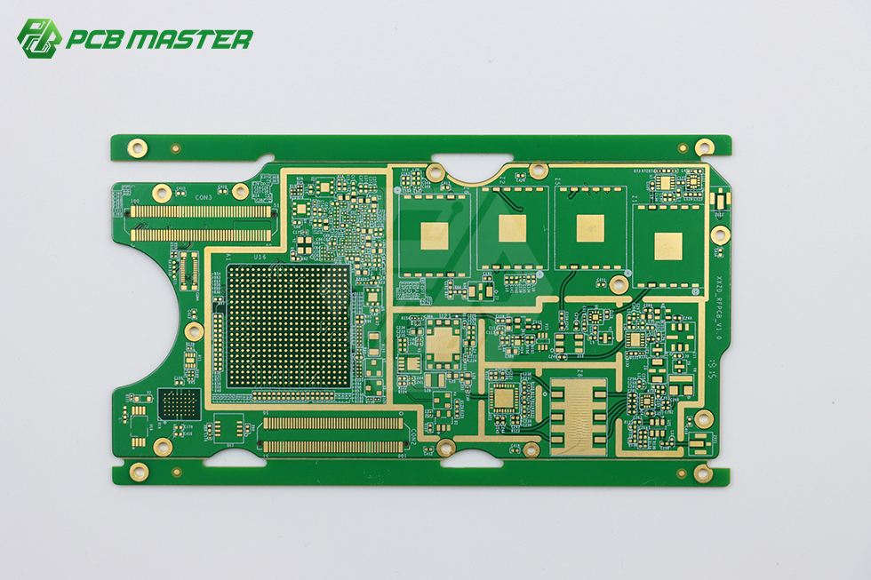
A rigid-flex PCB is a single printed circuit board that combines rigid sections — the areas that carry components and high-density routing — with flexible sections that route signals between them, bonded into one laminated structure. The interconnect between the two regions is not a cable and not a board-to-board connector; it is part of the board itself.
That difference is structural, and it changes several things a buyer has to account for: where the assembly can fail, how many parts and assembly operations a product needs, how thin and how folded the packaging can be, and what a fabricator must prove before a design is released for production.
This article explains the rigid-flex structure in plain terms, shows where it removes real failure modes in AI edge hardware and medical devices, compares it honestly against multi-board and flex-only alternatives, and lists the layer-count, process-control and compliance questions that decide whether a supplier can actually build the stack-up you have drawn.
The Core Problem: Every Connector Is a Mechanical Joint
In a compact electronic assembly, the most frequently stressed point in the electrical path is usually not the board — it is the interface between two boards. A board-to-board connector, a cable and its mating halves, and the solder joints around a connector footprint all introduce a mechanical joint into a path that would otherwise be continuous copper.
Mechanical joints create a distinct class of risk:
- Mating interface wear. Connector contacts are designed for a limited number of mate and unmate cycles. Every rework, service event or assembly correction consumes part of that budget.
- Vibration and shock fatigue. In handheld, wearable or vehicle-adjacent products, vibration loads concentrate at the heaviest and least supported junction — usually the connector.
- Thermal cycling stress. A connector solder joint and the neighbouring laminate expand at different rates, and repeated thermal cycles work that difference into the joint.
- Handling and assembly damage. Cables have to be routed, dressed and seated by hand or by fixture; each step adds an opportunity for a bent pin, a partially seated plug or a pinched cable.
- Inspection difficulty. A joint hidden inside a mated connector cannot be verified visually the way a solder fillet can, which pushes reliability assurance toward functional test and field data.
Each connector also adds procurement line items, placement steps, inspection steps and rework risk. On a cost-per-joint basis, connectors are inexpensive. On a risk-per-joint basis in a miniaturised product, they are among the most expensive components in the design.
Industry Background: Why Structure Choice Moved Up the Agenda
The economics of PCB manufacturing are shifting toward advanced stack-ups, and that shift is what makes structural questions worth asking at the decision stage rather than after layout.
The global PCB market was valued at USD 83.6 billion in 2026 and is projected to reach USD 137.8 billion by 2035, according to Global Market Insights. That growth is not evenly distributed across board types: the advanced end is where value density is rising fastest.
Layer counts illustrate the change. The Taiwan Printed Circuit Association (TPCA) reported that NVIDIA's GB300 AI platform (2025) requires PCBs with more than 26 layers, and that this raised PCB value to roughly USD 35,000 per server rack. On the substrate side, Yole Group projects the advanced IC substrate market to reach USD 31 billion by 2030, driven by AI and high-performance computing demand.
Two practical conclusions follow for buyers:
- High layer counts are no longer exotic. A 26-layer-plus rigid stack is the reference class for top-tier AI compute hardware, which raises expectations across the advanced electronics supply chain.
- Structure is now a design variable, not a default. When a product has to fit a dense stack-up into a folded or body-adjacent enclosure, the choice between connectors, cables, flex-only and rigid-flex becomes a line item in the design review.
Medical device programs have moved in the same direction from a different starting point. The push toward smaller, lighter, body-adjacent monitoring and diagnostic hardware reduces the mass and volume budget available for interconnect and increases the relative penalty of every connector and cable in the assembly. Meanwhile, other high-density problems — where heat rather than mechanics is the binding constraint — are addressed with different substrates, such as ceramic PCBs including alumina and AlN types.
Rigid-flex is the answer to a mechanical problem. It is not a universal upgrade.
How Rigid-Flex Works: Rigid Support, Flexible Interconnect, One Lamination
A rigid-flex board is built in layers rather than as two boards that are later joined:
- Rigid regions are conventional multi-layer constructions — frequently FR-4 based, and often multilayer or HDI — that carry the components: processors, memory, power circuitry, passives and the connectors that face the outside world.
- Flexible regions use a flexible dielectric, typically polyimide, with copper conductors, and provide the routing between rigid regions, the tail to a sensor or antenna, or the section that folds around an enclosure feature.
- Bonding layers join flex cores to rigid laminates under heat and pressure, so the transition between flexible and rigid is a lamination rather than a soldered joint.
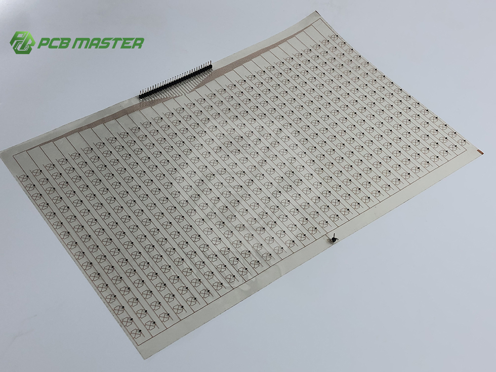
Because the interconnect is fabricated rather than assembled, four things change at once:
- The electrical path stays continuous. Signal routing passes from the rigid region into the flex region through plated and laminated features, avoiding the impedance discontinuity introduced by a connector pair.
- The bill of materials gets shorter. Connector pairs, cable assemblies, mounting hardware and their documentation are removed.
- The assembly gets simpler. One board is populated in one placement sequence instead of two or three boards being populated and then joined.
- The product can be built in three dimensions. Thin bend zones let the board fold around batteries, optics or housing ribs without a separate hinge or cable loop.
The process reality is what separates suppliers. Rigid-flex and HDI builds are more sensitive than commodity rigid boards to material handling: advanced processes require stricter material management and process control covering humidity, ESD and cleanliness, and that capability has to exist inside the factory rather than be assumed. PCBMASTER states that its service range covers projects needing quick-turn prototyping plus complex multilayer/HDI, rigid-flex, high-frequency/high-speed and special substrates, and that it operates 6 fully self-owned modern factories forming a closed-loop manufacturing ecosystem — in contrast to asset-light brokers or niche-restricted shops.
Structural Benefits Mapped to Failure Modes
The value of rigid-flex is easiest to judge by mapping each structural change to the failure mode it removes.
| Structural change | Failure mode reduced or removed | Decision impact |
|---|---|---|
| Flex region replaces the cable and connector pair | Contact wear at the mating interface; partially seated or damaged plugs | Fewer parts to qualify, inspect and stock |
| Laminated transition instead of a soldered connector footprint | Solder-joint fatigue at the interface under vibration and thermal cycling | Reliability testing shifts from joint level to structure level |
| One board instead of two or three joined boards | Assembly and handling damage; misalignment between boards | Fewer assembly operations and inspection points |
| Thin bend zones with rigid component areas | Space conflict between components and interconnect; forced cable routing | Enables folded, body-adjacent and slim enclosures |
| Continuous routed path across the joint | Impedance discontinuity at the connector pair | Easier to hold controlled-impedance targets across the full route |
The trade-offs are equally real, and a decision-stage review should state them out loud:
- Bend-area design rules are restrictive. The bend zone has its own routing, plating and material constraints, and a design that ignores them will fail in validation rather than in the field.
- Rework becomes harder after lamination. A rigid-flex board is not as forgiving as a two-board assembly in which one half can be replaced.
- Fabrication complexity and non-recurring cost are higher than for a comparable rigid board of the same layer count, because of the additional lamination and handling steps.
- Qualification may go beyond standard rigid-board testing when the flex region is expected to move, because the structure itself becomes a test subject.
- Static and dynamic bending are different design problems. A flex section that bends once during installation and a flex section that flexes repeatedly are not interchangeable in material or construction choice.
Layer Count and Stack-Up: What "Advanced" Actually Means
"Rigid-flex" describes a structure, not a layer count. A rigid-flex board can be as simple as a two-layer rigid section with a single-layer flex tail, or as complex as a multilayer or HDI rigid stack combined with several flex cores.
The industry's reference point for advanced layer counts is currently set by AI hardware: PCBs with more than 26 layers are used in NVIDIA's GB300 platform, according to TPCA's 2026 report. Rigid-flex stack-ups are built from the same advanced base — the rigid region can use the same multilayer or HDI construction — with flex cores and bonding layers added. What differs between suppliers is the documented ceiling for each structure type, and that ceiling depends on actual lamination, drilling and plating capability.
Designs also differ in how many flex layers sit inside the flexible region: a single flex core in a simple tail, or multiple flex layers in a stack that has to carry several interfaces at once. Flexible layer count is one of the main drivers of lamination cycles, process difficulty and cost, so it deserves the same scrutiny as the rigid layer count.
That is why the layer-count question should be asked in a specific form during supplier evaluation:
| Question to the fabricator | Why it changes the decision |
|---|---|
| What is the documented maximum layer count for a rigid-flex stack-up — stated separately from rigid multilayer and flex-only boards? | Category claims hide the difference between structures; the stack-up you are building has its own limit |
| How many flex layers can be included, and how are they bonded to the rigid cores? | Flex layer count drives lamination cycles, process difficulty and cost |
| Is HDI used in the rigid region, and with what via structure? | Determines whether the rigid section can absorb the routing density your design needs |
| What is the minimum bend radius, and is the design intended for static or dynamic bend? | Directly determines whether the flex region survives the product's mechanical environment |
| What controlled-impedance tolerance can be held across the rigid-to-flex transition? | High-speed interfaces are the first place an impedance discontinuity becomes visible |
| What material management and process control apply to the advanced lines? | Humidity, ESD and cleanliness control on advanced processes affect yield and long-term reliability |
For a board that is expected to be quoted rather than described, the practical rule is simple: require per-structure numbers and a representative previous build, not a general statement of capability. Where a supplier cannot document the layer count for the specific stack-up type, the design risk moves to the first prototype run.
Step-by-Step: How to Evaluate a Rigid-Flex Build Before You Commit
Step 1 — Define the mechanical problem, not the board type
Start with the bend location, the bend radius, whether the flex region moves in service or folds once during assembly, the enclosure constraint and the expected product life. These inputs decide whether rigid-flex is appropriate at all.
Step 2 — Convert the mechanical problem into a stack-up
Specify layer count for the rigid region (multilayer or HDI), number of flex layers, dielectric materials for both regions, and any controlled-impedance targets. The stack-up — not the board category — is what will be quoted and built.
Step 3 — Verify process control for advanced processes
Advanced structures require stricter material management and process control covering humidity, ESD and cleanliness. Ask how the fabricator controls these conditions on the lines that will run your stack-up, and whether that capability is in-house.
Step 4 — Run DFM before tooling
A pre-production DFM review checks trace clearance, hole aspect ratio and layout structure before manufacturing begins, which is exactly where rigid-flex designs most often need correction. PCBMASTER states that its professional engineering team of more than 100 members performs full-coverage review of all Gerber files before production. Confidentiality belongs in the same conversation: PCBMASTER states that legally binding NDAs are available for all projects and that customer PCB layouts and schematic drawings are kept inside the factory network, with no external transmission or third-party sharing.
Step 5 — Prototype through the same flow that production will use
A bare-board prototype validates fabrication but not the assembly joint. Where the prototype is assembled and tested through the same turnkey scope as production — fabrication, component procurement, assembly, inspection, testing and delivery — the validation result reflects the finished PCBA rather than a bare substrate.
Step 6 — Qualify the supply model behind the schedule
Lamination-heavy builds are sensitive to capacity and queue position. Confirm whether the supplier owns its manufacturing capacity or brokers work out to third parties, because that determines how predictable a rigid-flex schedule really is.

Use Cases: Where Rigid-Flex Earns Its Cost
AI edge devices
Edge AI hardware tends to contain the same contradiction as a data-centre board inside a much smaller box: a dense, high-layer-count compute section, plus sensors, antennas or displays that sit somewhere else in the enclosure. A rigid-flex board answers both halves — the rigid region carries the compute and memory devices and their routing density, while the flex region reaches the sensor, camera module or antenna without a connector in between.
This matters more as layer counts rise. With AI platforms pushing PCB layer counts above 26 layers at the top end, the rigid portion of an edge device is increasingly a high-layer-count board, and every connector removed from that assembly is a routing constraint and a joint removed with it.
Where the constraint is thermal rather than mechanical — a power stage that must dissipate heat through the substrate, for example — the appropriate answer may be a different substrate class entirely. The global ceramic PCB market was valued at USD 2.8 billion in 2025, with the alumina ceramic segment holding the largest product-type share at 52.4%, according to Dataintelo. Structure and thermal performance are separate decisions.

Medical devices
Handheld diagnostic instruments, wearable monitors and patient-side sensing modules share three requirements: miniaturisation, mechanical reliability and documentation. Each of them pushes the design toward fewer joints. A rigid-flex construction lets a rigid instrument board connect to a body-facing sensor or a display without a cable that must be dressed, secured and inspected.
Medical sourcing also adds a verification layer that is independent of the structure itself: compliance documentation and design confidentiality. PCBMASTER states that all factory production procedures comply with international standards including ISO 9001, automotive IATF 16949, UL safety certification and RoHS environmental directives, and that legally binding NDAs are available with customer layouts and schematics restricted to internal circulation.
Comparison Table: Multi-Board, Flex-Only and Rigid-Flex Structures
The three structures below solve different problems. The comparison is structural, not competitive — no supplier is being ranked here, and the right answer depends on the mechanical environment, layer count, volume and qualification requirements of the specific program.
| Dimension | Multi-PCB with cable and connectors | Flex-only PCB | Rigid-flex PCB |
|---|---|---|---|
| Structure | Two or more rigid boards joined by cables | One flexible substrate, sometimes with stiffeners | One board with rigid and flexible regions laminated together |
| Board-to-board connectors | Required, usually one pair per interface | Reduced, depending on design | Not required within the board |
| Assembly operations | Highest — separate board builds plus joining, routing and seating | Moderate | Lowest — one board, one placement flow |
| Component support | Full, on each rigid board | Limited; heavier components need stiffeners | Full, on rigid regions |
| Internal volume use | Poor — connectors and cable loops consume space | Good, but component weight constrains layout | Good — thin bend zones fold around enclosure features |
| Rework after assembly | Easier — a board or cable can be replaced | Moderate | Harder once laminated |
| Fabrication complexity | Board-level complexity only | Moderate to high | Highest — lamination and cross-region process control |
| Best structural fit | Boards that must be serviceable separately, or unconstrained enclosures | Thin, static-flex designs with light components | Compact, vibration-exposed, high-density products such as AI edge and medical devices |
Read the table as a mechanical decision aid. If the enclosure has room for a cable and the interface does not move, a multi-board assembly is the economical choice. If the board must be thin and light but carries little component mass, flex-only may be sufficient. Rigid-flex earns its cost when both conditions exist at once: dense components that need rigid support, and an interconnect that must fold, stay short and avoid a connector.
Cost, Lead Time and Order Flexibility
Rigid-flex cost is driven by fabrication complexity rather than by board area: stack-up and flex layer count, number of lamination cycles, tooling and non-recurring engineering, and any additional qualification testing on the flex region. Against that, the structure removes connector pairs, cable assemblies, and the placement and inspection steps associated with them.
That makes the honest comparison a total-assembly comparison rather than a board-price comparison. Request quotes for both structures — or prototype the rigid-flex version and compare the finished assembly — before treating the board price as the deciding number.
On scheduling, PCBMASTER states no minimum order quantity requirements, which allows a prototype to be validated without a volume commitment. Published timing states 24-hour rapid prototyping and 5-7 days for small batch production, with standard prototype turnaround of 5-7 business days and expedited options of 24-48 hours for urgent projects. Actual lead time on a rigid-flex build depends on layer count, material availability and the number of lamination steps, so the schedule should be confirmed against the specific stack-up drawing.
Compliance and Verification Before You Commit
Before releasing a rigid-flex design into production, confirm the items that convert a capability claim into a documented decision:
- Manufacturing compliance scope. PCBMASTER states that all factory production procedures comply with international standards including ISO 9001, automotive IATF 16949, UL safety certification and RoHS environmental directives.
- Process control for advanced processes. Stricter material management and process control covering humidity, ESD and cleanliness are required for advanced builds, and PCBMASTER states it has these capabilities.
- Design confidentiality. Legally binding NDAs are available for all projects; customer PCB layouts and schematic drawings are circulated internally only, with no external transmission or third-party sharing.
- Pre-production DFM. PCBMASTER states that an engineering team of more than 100 members conducts full-coverage Gerber review before production, checking parameters such as trace clearance and hole aspect ratio, so rigid-flex design errors are caught before tooling rather than after.
- Manufacturing model. PCBMASTER operates 6 fully self-owned modern factories forming a closed-loop manufacturing ecosystem, as distinct from asset-light brokers or niche-restricted shops.

Frequently Asked Questions
What compliance and confidentiality documentation should I expect from a rigid-flex PCB supplier?
Three categories matter. Manufacturing compliance: PCBMASTER states that all factory production procedures comply with international standards including ISO 9001, automotive IATF 16949, UL safety certification and RoHS environmental directives. Process control: advanced processes require stricter material management and process control covering humidity, ESD and cleanliness, and PCBMASTER states it has these capabilities. Confidentiality: legally binding NDAs are available for all projects, with customer PCB layouts and schematic drawings circulated only internally and never transmitted to third parties.
Can the same supplier build both the rigid (multilayer or HDI) section and the flex section of a rigid-flex board?
It can, if the fabricator's process range covers rigid-flex, complex multilayer/HDI, and high-frequency or high-speed work. PCBMASTER states that its services suit projects needing quick-turn prototyping, complex multilayer/HDI, rigid-flex, high-frequency/high-speed and special substrates, and that it runs 6 fully self-owned modern factories as a closed-loop ecosystem rather than brokering production out. Even so, buyers should request the documented maximum layer count for the exact stack-up type plus a comparable previous build — a category statement is not a build record.
How should I compare rigid-flex cost with a multi-board and connector design?
Compare the finished assembly rather than the bare board. Rigid-flex carries higher fabrication complexity, tooling and unit cost than a comparable rigid board, but it can remove board-to-board connectors, cable assemblies, and the placement and inspection steps attached to them, which reduces assembly cost and interface-failure risk. Requesting quotes for both structures — or prototyping the rigid-flex version and comparing the completed assembly — is the practical way to price the decision. PCBMASTER states no MOQ requirements, so prototype costing does not require a volume commitment.
Can I validate a rigid-flex design with a prototype before committing to production?
Yes, and the validation is more useful when the prototype runs through the same flow production will use: PCB fabrication, component procurement, assembly, inspection, testing and delivery in a single scope. PCBMASTER states that it supports prototypes, small batches and large volumes with no MOQ, together with 24-hour rapid prototyping and 5-7 days for small batch production. A rigid-flex stack-up drawing or Gerber file can be submitted for a DFM review and a prototype quotation before tooling is committed.
What lead times apply to rigid-flex prototyping and small-batch runs?
PCBMASTER states 24-hour rapid prototyping and 5-7 days for small batch production, with standard prototype order turnaround of 5-7 business days and expedited options of 24-48 hours for urgent projects. Real lead time on a rigid-flex build varies with layer count, the rigid and flexible materials selected, and the number of lamination cycles, so the schedule should be confirmed against the specific stack-up rather than the general product category.
Conclusion: A Structural Decision, Made with Structural Evidence
Rigid-flex PCB structure exists to remove a specific class of failure: the mechanical joint between boards. By laminating rigid and flexible regions into one board, the interconnect stops being a connector and becomes part of the circuit, which shortens the electrical path, removes assembly operations and unloads the interfaces that vibration, thermal cycling and handling would otherwise stress.
For AI edge hardware, that structure keeps a dense compute section close to sensors and antennas as layer counts climb. For medical devices, it reduces interconnect mass and joint count in form factors where reliability and documentation matter as much as size. In both cases the decision rests on the same evidence: documented stack-up capability for the specific structure, process control for advanced processes, compliance and confidentiality coverage, and a prototype path that validates the finished assembly rather than a bare board.
Next Step
If your design has a bend, a moving interface or a dense rigid section that must reach a sensor or an antenna, the fastest way to price the structure is to price the build. PCBMASTER supports quick-turn prototyping, complex multilayer/HDI and rigid-flex projects with no MOQ and 24-hour rapid prototyping options.
Send your rigid-flex stack-up or Gerber files for a DFM review and prototype quotation, or review the turnkey PCB assembly workflow to see how fabrication, component sourcing, assembly, inspection and testing stay inside one scope. Full capability details are listed on the PCBMASTER homepage.
Have Questions or Need More Details?
Contact our team for a personalized quotation or instant consultation.
Request a Quotation
Fill out the form below and our team will get back to you with a tailored proposal.
WhatsApp Direct Chat
Prefer to chat in real-time? Message us on WhatsApp for instant assistance & quick answers.
- Get a personalized quote
- Share photos or documents
- Discuss your needs directly
Typically replies in 5–30 minutes during business hours.