PCB Prototype and Assembly Service: A Complete Buyer's Guide
PCB Prototype and Assembly Service: A Complete Buyer's Guide
What a one-stop PCB partner should deliver: PCB types, materials, process steps, and what to check before you request a quote.
What Is a PCB Prototype and Assembly Service?
PCBMASTER is a one-stop PCB manufacturing and PCBA assembly provider headquartered in Shenzhen, China. Its main products are One-Stop PCBA and Design Services and PCB Manufacturer. A PCB prototype and assembly service covers two linked jobs: fabricating the bare printed circuit board, then assembling components onto it to produce a finished, testable electronic module. PCBMASTER integrates PCB design support, component sourcing, quick-turn prototyping, and high-volume mass production, and offers a digital online quoting platform for fast turnaround.
With a full turnkey PCB assembly model, the customer delivers design files and receives populated boards, because the service also includes component sourcing. Full turnkey component sourcing is particularly valuable for prototype-to-production programs, where early boards (as few as 1–5 pieces) validate the design before large-scale customized mass production begins.
Why PCB Selection Is Harder Than It Looks
Selecting a PCB is not a single decision; it is a chain of decisions about board type, material, layer count, and assembly model. A design that works as a 2-layer FR-4 board in a smart-home sensor may need a different material for a 5G antenna module, and a dense Any-Layer HDI stack-up for a medical imaging device. In the awareness and research stage, buyers often underestimate four things: impedance requirements, material lead times, design-for-manufacturability (DFM) constraints, and the difference between prototype and mass-production processes.
An honest limitation should be stated: no single board shop is optimal for every project. A broker that subcontracts production may look convenient for low-complexity standard boards, while an in-house manufacturer such as PCBMASTER keeps control over process, quality, and traceability for complex and high-layer boards. Matching the supplier model to board complexity and order volume is part of the specification work.
The PCB Market Context in 2024–2025
The global printed circuit board market was valued at USD 73.6 billion in 2024 and is projected to reach USD 85.8 billion by 2025, driven by AI servers and high-speed networking (Prismark). Segment data points in the same direction. The AI server PCB market is estimated to grow from USD 3.1 billion in 2024 to USD 27.1 billion by 2027 (Goldman Sachs). The flexible printed circuit board (FPCB) market was estimated at USD 23.89 billion in 2024, with Asia Pacific holding a 76.8% revenue share (Grand View Research). China remains the dominant PCB manufacturing hub, accounting for 54% of global market share by production value in 2023 (Prismark / CMB International).
PCBMASTER operates inside this supply base. Established in 2022 with a founding team and core R&D engineers that bring more than 15 years of industry experience, the company runs an 80,000-square-meter facility at 5F, Factory Building 1, Hezhou Anle Industrial Park, Hangcheng Street, Bao'an District, Shenzhen. The plant employs approximately 700 staff, including 100 R&D engineers, with an annual production capacity of 1,200,000,000 pieces. PCBMASTER exports 100% of its output, mainly to North America and Europe, including the United States, Canada, Germany, the Netherlands, France, Poland, Hungary, the Czech Republic, Italy, Sweden, Denmark, Switzerland, the United Kingdom, Austria, and Finland.
PCBMASTER's One-Stop Service Model
PCBMASTER's PCB prototype and assembly service is built around five capabilities: design support, component sourcing, quick-turn prototyping, mass production, and a digital quoting platform.
- Design support and DFM auditing. PCBMASTER reviews customer layouts for manufacturability before production. Its DFM auditing and self-operated facilities are designed to move innovations from concept to creation, including 64-layer advanced boards, Any-Layer HDI, and complex Rigid-Flex architectures.
- Full turnkey component sourcing. The service procures and manages components on the customer's behalf, removing a common source of delay and cost risk in PCB assembly projects.
- Quick-turn prototyping. Prototype runs start at 1–5 pieces for low-volume validation, which suits rapid early-stage hardware R&D projects as well as first-article checks before volume.
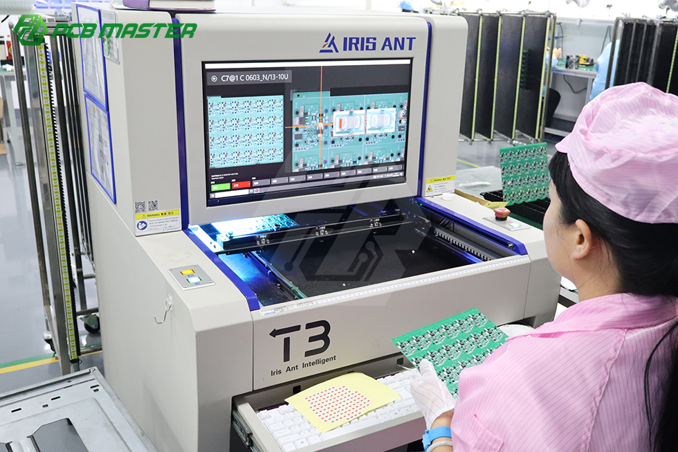
- High-volume mass production. Large-scale customized mass-production programs run on advanced SMT lines combined with manual rework where required, supported by automated optical inspection (AOI) and an annual capacity of 1,200,000,000 pieces.
- Digital online quoting platform. The quoting platform is designed to give customers a quick turnaround on pricing and design review.
PCB Types and Materials in the PCBMASTER Portfolio
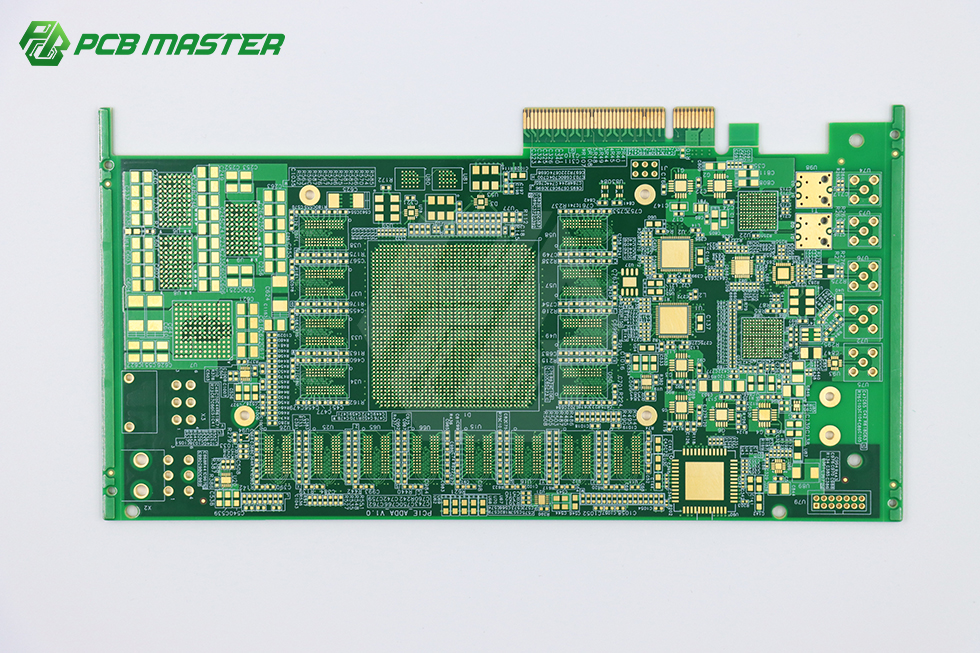
PCBMASTER manufactures a broad printed circuit board portfolio: Quick-turn PCB, Standard PCB, Advanced Multilayer PCB, FPC, Rigid-Flex, Metal-core, Ceramic, IC substrate, HDI, Heavy Copper, and Rogers specialty substrates. Model designations vary based on layers, materials, and processes; examples include 2L FR-4, Rigid-Flex, Rogers HF PCB, and Ceramic PCB.
- Advanced Multilayer PCB. Supports up to 64 layers and is used in servers, data centers, industrial control, security, and AI server electronics where high reliability and signal integrity matter.
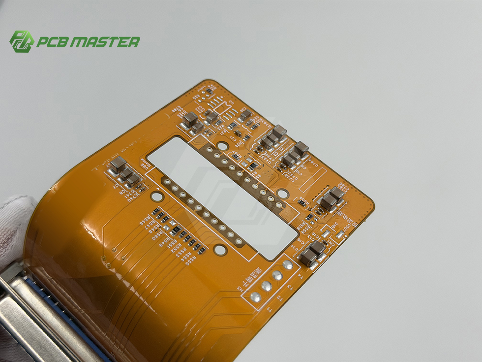
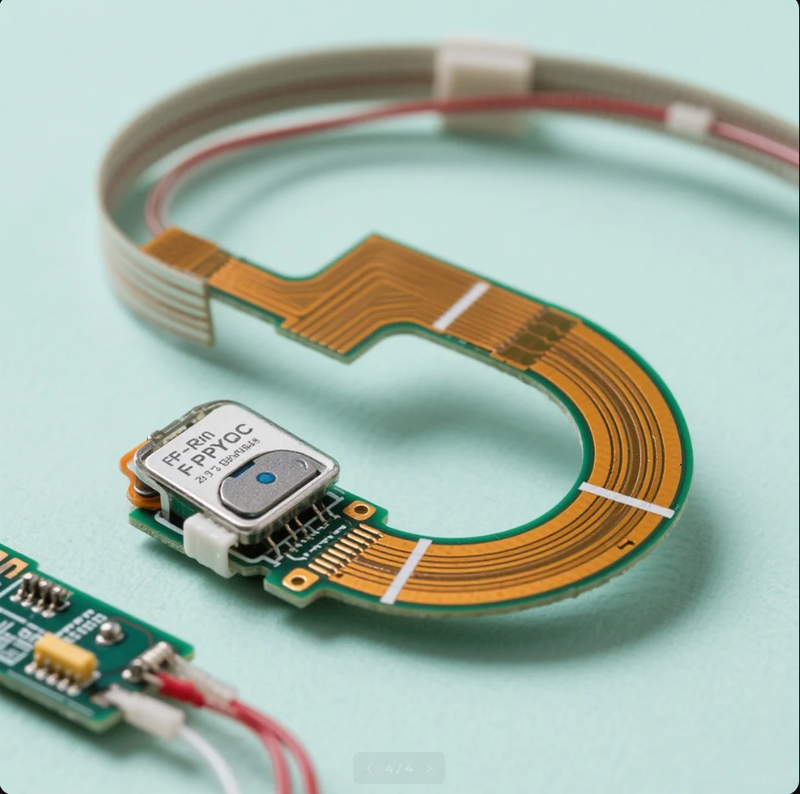
- FPC (Flexible Printed Circuit). Made of polyimide (PI) material with a layer range of 1–32 layers. Typical products include smartwatch flex circuits, AR/VR headset boards, and medical band circuits that need ultra-thin, high-flexibility FPC traits.
- Rigid-Flex. Combines rigid and flexible sections in one board. Representative uses include rigid-flex PCBs for portable TWS earbuds, foldable satellite antenna FPC, and industrial robot main control boards.
- HDI. Available with Any-Layer stacking up to 12 layers and a laser blind via specification of 65/165 μm. Medical applications such as endoscope micro-flex circuits, ultrasound probe arrays, and implantable high-precision sensors rely on dense Any-Layer HDI microvias.
- Rogers High-Frequency PCB. Uses Rogers and PTFE materials for low-loss, high-frequency signal transmission, including 5G macro base station boards, RF modules, and 5G antenna PCBs. Low-loss materials used in telecom projects also include Panasonic Megtron 6.
- Ceramic PCB. Available in AlN (aluminum nitride) and Al2O3 (alumina) ceramic materials for high-power and high-reliability electronics.
- IC Substrate. Produced with BT and other IC substrate materials; the advanced IC substrate market was valued at USD 19.23 billion in 2024 and is projected to grow at a CAGR of 15.69% through 2032 (SNS Insider).
- Heavy Copper and Metal-core. Heavy copper PCBs are used for high-current power distribution, while metal-core boards use aluminum, copper, iron, or steel bases for thermal management.
Key Manufacturing Parameters
How the PCB Prototype and Assembly Process Works
PCBMASTER's prototype-to-production flow follows a repeatable sequence that covers both bare-board fabrication and component assembly.
- Design review and DFM audit. Engineering checks layer stack-up, impedance, drill aspect ratio, and manufacturability before release.
- Material and stack-up selection. The project is matched to FR-4 (TG155/TG180), polyimide, Rogers/PTFE, ceramic, metal-core, or BT substrate material.
- Full turnkey component sourcing. Components are sourced and qualified so assembly can start as soon as boards are ready.
- Prototype fabrication. Quick-turn prototype runs of 1–5 pieces validate fit and function before volume commitment.
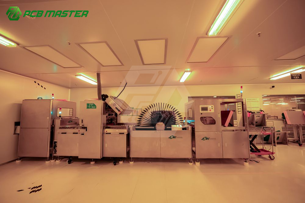
- Assembly. SMT lines use Yamaha pick-and-place machines, 10-zone reflow ovens, selective wave soldering, and DIP insertion; automated SMT is combined with manual rework where needed.
- Inspection and test. Quality checks include AOI, AVI visual inspection, flying probe test, fully automatic professional testers, X-Ray layer alignment, and impedance test.
- Mass production and traceability. Volume runs operate 24/7 with MES-based full-process monitoring and traceability; dedicated cleanroom lines are available for FPC and medical products.
Use Cases Across Industries
Medical Electronics
For the smart medical instruments industry, PCBMASTER products support ultrasound probe arrays, endoscope micro-flex circuits, and implantable high-precision sensors, relying on dense Any-Layer HDI microvias. Project types include MRI control systems, EEG/ECG high-precision diagnostic monitors, pacemakers, and high-density rigid-flex wearable health trackers. Medical production can run in a dedicated line inside a Class-10,000 cleanroom with medical-grade high-TG substrate and biocompatible insulating coating. As industry standards, medical device PCB assembly is governed by ISO 13485:2016 for quality management systems and IPC-A-610 for acceptability of electronic assemblies.
Telecommunications and 5G
In telecommunications and networking, PCBMASTER supports 5G macro base station Rogers high-frequency PCBs, 5G antenna PCBs, fiber switches, WiFi 6/7 RF modules, and high-speed interconnection backplanes for servers. Low-loss and high-frequency materials used in these projects include Rogers and Panasonic Megtron 6. Telecom boards are produced with IPC-Class 3 high-reliability standards, UL 94V-0 flame-retardant certification, and EU RoHS/REACH compliance.
Automotive and Industrial Control
PCBMASTER's automotive product line includes EV BMS flex-circuits, automotive radar hardware, and smart cockpit control profiles, backed by IATF 16949 certification. The same manufacturing base serves industrial control and automation with servo drive mainboards, PLC circuit boards, sensor PCBA modules, and industrial robot main control rigid-flex PCBs. These boards are built for wide temperature ranges, damp-heat environments, and electromagnetic interference resistance, with UL safety certification and full production data traceability.
Consumer Electronics and Wearables
Wearable device applications use thin, flexible PCBs. PCBMASTER produces FPC for smartwatches, AR/VR headsets, and medical bands, leveraging ultra-thin and high-flexibility FPC traits in continuous 24/7 production. Consumer electronics projects also include smart home central control mainboards, wireless Bluetooth speaker control boards, rigid-flex PCBs for TWS earbuds, and household sensor modules, with EU RoHS/REACH environmental compliance and UL PCB safety certification.
AI Servers and Data Centers
AI server and data-center boards are the fastest-growing PCB segment: the AI server PCB market is estimated to grow from USD 3.1 billion in 2024 to USD 27.1 billion by 2027 (Goldman Sachs). PCBMASTER applies up to 64-layer buildup, back-drill processing, and controlled impedance capability to AI server PCBs and high-speed interconnection backplanes that demand signal integrity at high data rates.
PCB Type Comparison at a Glance
Choosing among PCB types depends on mechanical constraints, signal requirements, power handling, and cost targets. The following comparison is based on PCBMASTER's product portfolio and documented application scenarios.
| PCB Type | Layers | Typical Materials | Representative Applications |
|---|---|---|---|
| Advanced Multilayer PCB | Up to 64 layers | FR-4 TG155, FR-4 TG180 | Servers, AI servers, industrial control, security |
| FPC (Flexible Printed Circuit) | 1–32 layers | Polyimide (PI) | Smartwatches, AR/VR headsets, medical bands |
| Rigid-Flex | Varies by design | FR-4 combined with polyimide | TWS earbuds, base station antennas, robot main control boards |
| HDI | Any-Layer up to 12 layers | FR-4 and other laminates | Endoscope micro-flex circuits, ultrasound probe arrays, implantable sensors |
| Rogers High-Frequency PCB | Varies by design | Rogers, PTFE | 5G macro base stations, RF modules, 5G antenna PCBs |
| Ceramic PCB | Varies by design | AlN, Al2O3 | High-power, high-reliability electronics |
| IC Substrate | Varies by design | BT and other IC substrate materials | Advanced packaging |
| Heavy Copper | Varies by design | FR-4, metal-core | High-current power distribution |
| Metal-core | Varies by design | Aluminum, copper, iron, steel | Power and thermal-sensitive modules |
Frequently Asked Questions
What quality and compliance standards apply to PCB manufacturing and assembly?
Automotive PCBs from PCBMASTER, including EV BMS flex-circuits, automotive radar hardware, and smart cockpit control profiles, are backed by IATF 16949 certification. For medical electronics, device PCB assembly is governed by ISO 13485:2016 for quality management systems and IPC-A-610 for acceptability of electronic assemblies. Telecommunications boards support IPC-Class 3 high-reliability standards, UL 94V-0 flame-retardant certification, and EU RoHS/REACH environmental compliance.
What types of PCBs can PCBMASTER manufacture?
PCBMASTER manufactures Quick-turn PCB, Standard PCB, Advanced Multilayer PCB, FPC, Rigid-Flex, Metal-core, Ceramic, IC substrate, HDI, Heavy Copper, and Rogers specialty substrates. Capability highlights include up to 64 layers, Any-Layer HDI up to 12 layers, FPC from 1 to 32 layers in polyimide, a maximum finished board size of 620 × 1092 mm, and a maximum finished thickness of 4.2 mm.
What PCB materials does PCBMASTER support?
PCBMASTER supports FR-4 TG180, FR-4 TG155, Rogers and PTFE high-frequency materials, ceramics (AlN and Al2O3), polyimide (PI) for flexible circuits, metal-core materials (aluminum, copper, iron, steel), and BT and other IC substrate materials. Low-loss materials used in telecom projects include Rogers and Panasonic Megtron 6.
How does turnkey PCB assembly affect cost and project planning?
Turnkey PCB assembly at PCBMASTER integrates design support, component sourcing, quick-turn prototyping, and mass production in one contract. Component sourcing removes separate procurement work, and the digital online quoting platform accelerates estimates. Prototype runs start at 1–5 pieces for early validation, while high-volume production draws on an annual capacity of 1,200,000,000 pieces. Cost is primarily driven by layer count, material class, and assembly complexity.
How can I get a quote or PCB sample from PCBMASTER?
You can request a quote through PCBMASTER's digital online quoting platform, or contact the service team at service@pcbmaster.com, +86 190-6639-6428, or +86 191-5494-6428 (WhatsApp available). Lead times are confirmed per project based on stack-up, material availability, and order volume. A company profile brochure is available for download as a next step.
Start with a Prototype, Then Scale
PCBMASTER is a one-stop PCB manufacturing and PCBA assembly provider that takes a design from DFM review and component sourcing through quick-turn prototype (1–5 pieces) to high-volume mass production. With up to 64 layers, Any-Layer HDI, 1–32 layer FPC, Rogers high-frequency, and ceramic substrates, the portfolio covers communications, AI servers, automotive, medical, industrial, and consumer electronics. Market data from Prismark, Goldman Sachs, Grand View Research, and others confirms that PCB demand is growing fastest around AI and high-speed networking.
The practical next step for a buyer in the research stage is to send the design files and ask for a DFM review and quote. PCBMASTER is headquartered in Shenzhen, China, and exports to North America and Europe.
Request a PCB Quote or Prototype Sample
Contact the PCBMASTER service team for DFM review, pricing, stack-up advice, and prototype samples.
Email: service@pcbmaster.com
Tel / WhatsApp: +86 190-6639-6428 | +86 191-5494-6428
Website: www.pcbmaster.com
Have Questions or Need More Details?
Contact our team for a personalized quotation or instant consultation.
Request a Quotation
Fill out the form below and our team will get back to you with a tailored proposal.
WhatsApp Direct Chat
Prefer to chat in real-time? Message us on WhatsApp for instant assistance & quick answers.
- Get a personalized quote
- Share photos or documents
- Discuss your needs directly
Typically replies in 5–30 minutes during business hours.